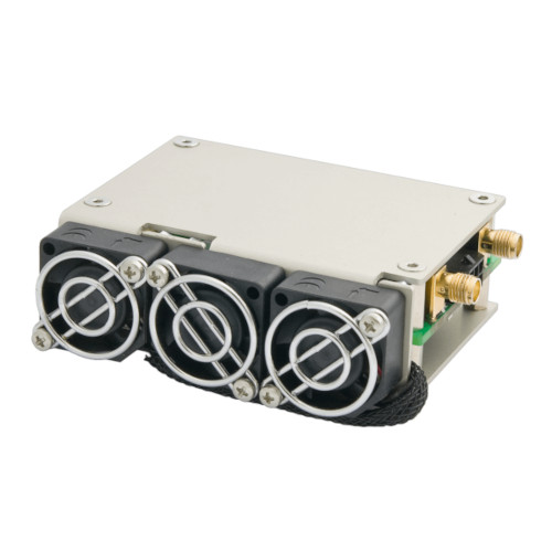
QBY-BT GaN Pockels cell driver is encased version of QBY-4001 board with comfortable user interface and may be used for advanced beam control: advanced q-switching, beam slicing, pulse picking, regenerative amplifiers control
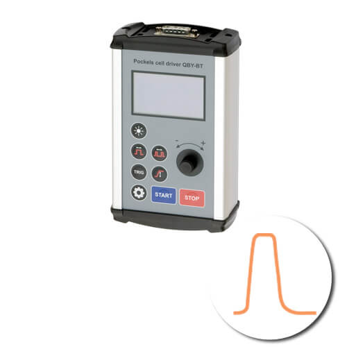
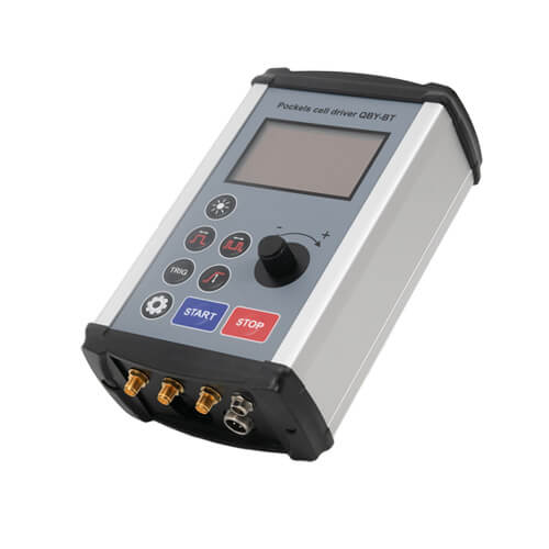

Universal driver, suitable for advanced q-switching, beam slicing, pulse picking, control of regenerative amplifiers.
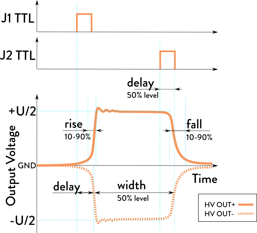
QBY-BT is an encased version of QBY-4001 board, easy for the user to mount and use. It runs on 24 V DC. The voltage level, operating frequency and pulse width can be selected in working range by user through RS-485 or through the front panel. Pulse controlling TTL signals J1 and J2 (see the picture below) are generated internally under controller regulation, simultaneously the module generates an output synchronisation signal (TRIGGER OUT) with a definite time shift towards to J1, this could help to syncronise the whole system. It is also possible to connect an external pulse generator to set an operating frequency and pulse width.
The fact that the drivers have a big number of settings, allowing an output signal customization in many ways to solve wide range of tasks, makes them very suitable to use in laboratory.
Output voltage is up to 4 kV, max. rep. rate strongly depends on selected output voltage value and on load capacitance (we recommend therefore to use the shortest possible cables and choose a Pockels cell with lower capacitance). In order to keep its performance close to datasheet values, one needs to minimize the load capacitance, numbers less than 5 pF are appreciated.
Please, note that by bipolar device an output pulse voltage U is formed by applying +U/2 to positive output wire and –U/2 to negative.
The module was designed to work in set-reset scheme when a base voltage level equals to zero. Non-periodic pulses are also possible, set by pulse generator.
QBY-BT is based on GaN transistors and offers fast transition time for both pulse edges (3-4 ns).