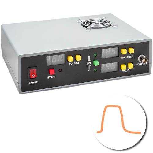
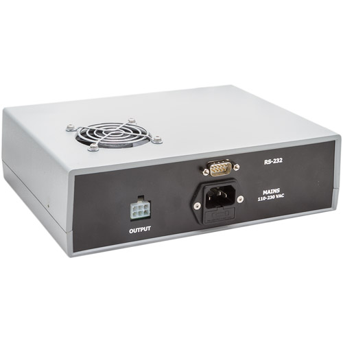
QBU-BT-series are encased version of QBU boards, easy for the user to mount. They run on common 100-240 V AC 50/60 Hz, so, you don't need extra power supply for the driver. The voltage level, operating frequency and pulse width can be selected in working range by user through RS-232 or through the front panel. Triggering is carried out automatically or via a signal from an external device.
The fact that the drivers have a big number of settings, allowing an output signal customization in many ways to solve wide range of tasks, makes them very suitable to use in laboratory.
Different operating modes by output signal form are possible:
• push-up (= normally off scheme), when a base voltage level equals to zero, triggering is internal
• pull-down (= normally on scheme), when pulses are generated from base bias voltage to ground, triggering is internal.
• user-defined scheme, with arbitrary width and frequency of pulses, triggering by an external low voltage arbitrary TTL signal, external synchronization mode
QBU-BT-series is based on MOSFET technology and offers high repetition rates and fast transition time for both pulse edges (< 15 ns).
Input:
Output:
pull-down scheme
push-up scheme
triggering by an arbitrary external TTL signal
HV high level (pulse amplitude)
adjustable in HVMIN – HVMAX range (see also Modifications section), up to 6 kV1
HV low level (pulse basement)
fixed, 0 V
Pulse width
1 us - 1/f (f is repetition rate in Hz) in internal synchronization mode
200 ns - DC (in external synchronization mode)
Maximum repetition rate
up to 100 kHz 1 and higher (load and voltage dependant, see also manual)
Rise / fall time
< 15 ns 2
Protection
from overheating (approx. 72 °C)
Environment:
Operation temperature
0 … +40 °C (wider temperature range is available on request)
Storage temperature
-20 … +60 °C
Humidity
0 ... 90%, non-condensing
Other:
Size (LxWxH)
225x180x70 mm
1)
these parameters aren't indepenent and cannot achieve their maximum at the same time
2)
10-90% level, guaranteed at load capacitance 11 pF and below
Modifications
QBU-XXYY-LJ-[ZZZ], where:
- XX codes the maximum possible output voltage (HVMAX, user selectable up to 6000V),
- YY codes the minimum HV output voltage level (HVMIN, 40% of HVMAX)
- LJ – low jitter option (supplied by default). The LJ version of the driver jitter is as low as ±1ns, the delay time is shorter than 100ns.
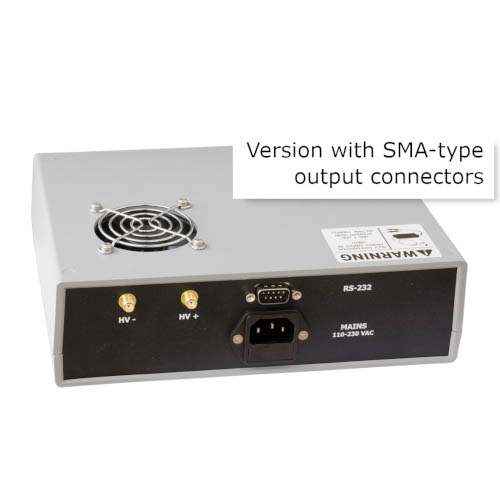
- ZZZ codes optional version different with output connectors:
SMA – version of the product with SMA-type output connectors (see Manual for the details), available only for low voltage versions of the product (1500V and below), suitable for driving of unipolar Pockels cells of low capacitance (e.g. EO phase and amplitude modulators).
2.4-6.0 kV high voltage adjustment range
2.0-5.0 kV high voltage adjustment range
1.6-4.0 kV high voltage adjustment range
1.2-3.0 kV high voltage adjustment range
0.8-2.0 kV high voltage adjustment range
QBU-BT-1506-LJ
QBU-BT-1506-LJ-SMA
0.6-1.5 kV high voltage adjustment range
QBU-BT-1004-LJ
QBU-BT-1004-LJ-SMA
0.4-1.0 kV high voltage adjustment range
(*) Other output voltages are available on request
Example
2.0-5.0 kV high voltage adjustment range